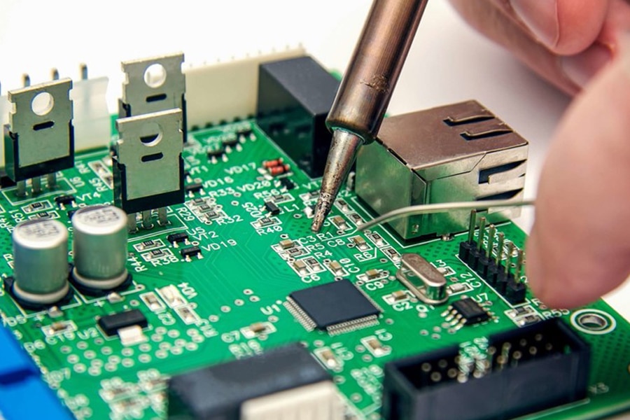
If you’re one of our electronics enthusiasts friends, you’ve probably heard how devices become faster as they shrink in size. High-Density Interconnect (HDI) PCBs are a big part of that trend. These PCBs pack a lot into a tiny space and use Surface Mount Technology (SMT) to handle high-performance components on super-tight layouts.
But making HDI and SMT work together takes more than just shrinking everything down. The secret lies in designing vias and pads that fit both the HDI format and the SMT requirements, so everything functions smoothly without a hitch. Here’s a look at what that involves, with some cool, handy tips to help get it right.
Why Via and Pad Design Matter in HDI PCBs
Vias and pads are the connectors and anchors of any PCB. Vias carry signals between the different layers, while pads hold components in place on the surface. When you’re dealing with HDI designs, space is at a premium, so every via and pad has to be spot on. Mess them up, and you’re looking at all sorts of issues—signal interference, unreliable connections, and maybe even physical breaks in the board.
For SMT, you’ve got to make sure your vias and pads don’t just fit but also handle high-speed signals, manage heat, and survive the manufacturing process. There’s a lot riding on these tiny design choices!
Types of Vias Used in HDI PCBs
In HDI PCBs, designers use a few types of vias to maximize space and manage signal flow. Here’s a quick rundown:
Microvias
These little guys are laser-drilled holes that connect nearby layers. Because they’re small (under 150 micrometers in diameter), they take up way less room than standard vias, making them ideal for tight HDI layouts. Microvias are super helpful when you need to save space without skimping on performance.
Blind Vias
Blind vias connect outer layers to one or more inner layers but don’t go through the whole board. They’re awesome for HDI because they don’t take up as much vertical space, leaving more room for other stuff on the board.
Buried Vias
Buried vias only connect inner layers, staying completely hidden inside the board. They’re perfect for keeping top and bottom layers clear, which is handy when you’re dealing with high-density layouts.
Tips for SMT-Compatible Pads in HDI Designs
Pads anchor the components to the PCB. If your pad design is off, you’ll run into soldering issues or end up with weak connections—definitely not what you want in a dense HDI setup.
Get the Pad Size and Shape Right
Your pad size needs to match the component footprint, especially in HDI designs where space is tight. Too big, and you risk solder bridging; too small, and you’ll get weak connections. Matching the pad exactly makes assembly smoother and gives you a reliable solder joint.
Pick Between SMD and NSMD Pads
There are two main types of pads: Solder Mask Defined (SMD) and Non-Solder Mask Defined (NSMD). NSMD pads are usually the favorite because they give a cleaner solder joint and more control over pad dimensions. But SMD pads have a bit more strength, which can help in certain high-density builds.
Try Via-in-Pad Design
Via-in-pad places microvias right inside the component pad, creating shorter signal paths and improving high-frequency performance. This setup is really useful in HDI designs where space is limited. Just remember to fill and plate those vias. Otherwise, solder can seep into the hole during assembly and cause a weak connection.
Best Practices for Via Design in SMT-Compatible HDI PCBs
Smart Via Placement
Good via placement can prevent problems like crosstalk (when signals jump into each other’s lanes) and signal loss. Keep vias away from high-speed traces to reduce interference, and cluster them in areas with lower signal activity when you can.
Use Stacked or Staggered Microvias
Stacked microvias are all lined up vertically across multiple layers, which works well for straight connections. Staggered microvias, on the other hand, are offset between layers, giving the board more strength. Choose based on what your circuit board design needs most—direct connections or added durability.
Thermal Vias for Heat Control
HDI boards, especially with a lot of components, can run hot. That’s where thermal vias come in. They help move heat away from hot spots by channeling it to other layers or heat sinks. Properly placed thermal vias keep your board’s temperature in check, which is a huge plus for the lifespan of sensitive components.
Material Choices and Manufacturing Tips
Use High-Tg and Low-Loss Materials
HDI boards in high-frequency designs need materials that can handle high temps and reduce signal loss. High-Tg (glass transition temperature) materials resist the intense heat during SMT processes. Low-loss materials keep signal quality sharp, so they’re worth the investment for complex designs.
Ensure Reliable Vias with Fill and Plating
For via-in-pad designs, filling and plating vias is a must. This step creates a smooth surface for soldering, which makes for a strong connection. Sure, it costs a bit more. However, it’s really worth it if you’re aiming for quality.
Keep an eye for more latest news & updates on Uniquei Tech!


